CNRS UMR137/Thales is one leading research lab in Europe and a joint laboratory between CNRS and the industrial company Thales (previously Thomson-CSF), associated with University Paris-Saclay. UMPhy led the first discovery of the GMR in 1988 whose major importance was recognized by the 2007 Physics Nobel prize. Main Expertise: Initially centered on spintronics and nanomagnetism, the scientific activities were extended in 1996 to High-Tc superconductors (HTCS).
Project Leader:
Dr. Javier Briatico
CNRS Senior scientist
head of the group “HTc superconductors and signal treatement” Unité Mixte de Physique CNRS/Thales
Research interests and expertise: Thin films deposition, High Tc Superconductors, Electric transport, Magnetic properties, Optical lithography, Multiferroic and Superconducting device elaboration, Radio Frequency, Microwaves
Contact: javier.briatico(at)cnrs-thales.fr
Team:
Dr. Javier Villegas
CNRS Senior scientist – Unité Mixte de Physique CNRS/Thales
Research interests and expertise: High Tc Superconductors, Vortices, Electric transport, Magnetic properties, Superconducting Hybrids
Contact: javier.villegas(at)cnrs-thales.fr
Dr. Anke Sander
CNRS Engineer – Unité Mixte de Physique CNRS/Thales
Research interests and expertise: Thin films deposition, High Tc Superconductors, Hybrid structures, Transport characterization, Structural characterization, AFM, SEM, XPS
Contact: anke.sander(at)cnrs-thales.fr
Dr. Karim Bouzehouane
CNRS Engineer – Unité Mixte de Physique CNRS/Thales
Research interests and expertise: Near-Field Microscopy, AFM, CAFM, Nano-Indentation
Contact: karim.bouzehouane@cnrs-thales.fr
Santiago J. Carreira
Post-Doc (Marie Skłodowska-Curie Actions)
Research interests and expertise: High Tc Superconductors, Vortices, Electric transport, Magnetic properties, Superconducting Hybrids, Ferromagnetic resonance.
Contact: santiago.carreira@cnrs-thales.fr
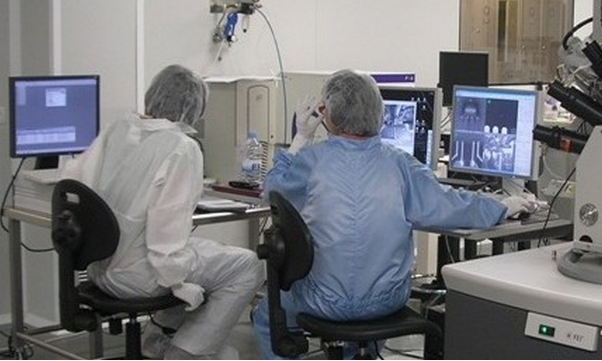
Equipment
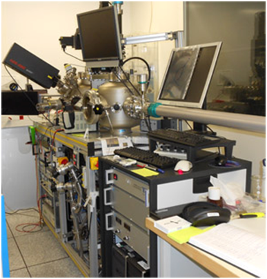
Pulsed Laser Deposition System REAL
In this pulsed laser deposition system, UV (248 nm) light from a class IV laser is focused inside a vacuum chamber to vaporize atoms from a ceramic target of the material to be deposited. Atoms deposit as a thin film on a substrate heated at high temperatures.
A large number of growth parameters can be controlled during deposition: Oxygen partial pressure, substrate temperature (from 30 °C up to 750 °C), substrate-target distance (from 40 to 90 mm), laser energy (up to 600 mJ) and frequency (max 50 Hz). The system supports 4 targets, so a large variety of structures can be growth “in situ”. Samples of thickness from 2nm up to 500 nm are usually deposited on substrates of 10mmx10mm.
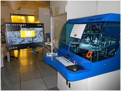
Clean Room facilities
Optical lithography comprises all lithographic techniques to fabricate microdevices using top-down techniques. The lab dispose of two different optical technologies: a Mask Aligner (MJB3) and a 2D laser lithography. Our insulator deposition machine (SiO2 or Si3N4), and the Ion Beam Etching and Reactive Ion Etching machines provide the necessary steps for the elaboration of devices in the “current perpendicular to the plane” configuration.
Transport Measurement
Different Transport Measurement setups are available in our lab, to measure the resistance and the complex impedance of films and devices, in the range of temperatures between 12K and 300K, from DC to 30 GHz, up to 6 KGauss.